AN ISO 9001 : 2008 CERTIFIED CO
AN ISO 9001 : 2008 CERTIFIED CO
In 1925 Charles duccas submitted a patent of electric path directly on an insulated surface, it was first PCB design in history. PCB was not popular back than but it was a revolutionary idea because it could eliminate complex wiring and provide consistent result. After 1950 PCB became popular for circuit and electronics and so many changes came to design and its process but vat polymerization process of 3D printing is going to add new dimension in PCB manufacturing.
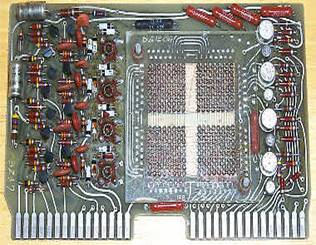
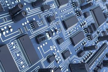
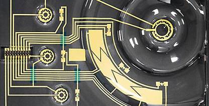
In 3D printing you can add traces of gold or copper into model and create path for your electric device, it is called molded interconnect device (MID). Key markets for MID are consumer electronic, telecommunication, automotive and medical. A very common application for MIDs are integrated antennas in cellphone.
Molded interconnect devices are manufactured using Laser Direct Structuring (LDS), in which laser activate the metallic inorganic compound. After that in electroless copper bath layers arise precisely on these tracks. So, LDS process involve mainly three process
1) injection molding,
2) Laser structuring,
3) electro plating therefor it offers lower tools and equipment cost than other technique.
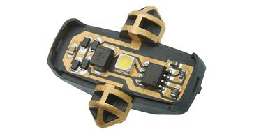
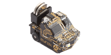
Traditional PCB can’t be placed In compact size machine so to make device sophisticated small two worlds of mechanical and electrical need to come together to meet demand of our compact and complex design.
Application:
There are many devices in market that uses MIDs technology to achieve their function while consuming minimal space like automotive, medical, space and satellite, gadgets and of course in IOT application.
1) Automotive
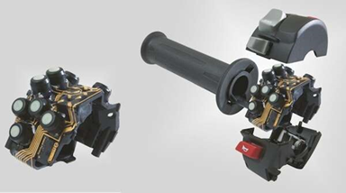
Automotive sector is using lots of sensors nowadays to get accurate data of vehicle and passenger and MIDs is helping by providing perfect mechatronics device.
2) Medical
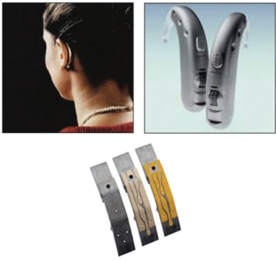
Medical sector is facing challenges of electrical device or sensor that can perfectly fit on body according to shape of surface and sometimes in surgery doctors also need sensor to check the status of patient by inserting the sensor in patient. Doctors need sensor in different shapes so it can fit or travel through human body in mean time collect data and send back to device therefor MIDs are opening new doors for medical sector.
3) Gadgets
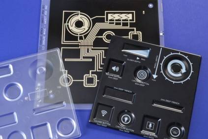
Every day we use electronic appliances like smart watch, smart tv, audio – video players and others. We like them to be compact and more powerful but to achieve that they need to organize more component in less space. In traditional PCB designers has limits to arrange their components in single side or both side they can’t arrange them in other surface but using MIDs designers can place component in any surface they want and develop gadgets more powerful than ever before.
MIDs is the future of both electrical and mechanical engineer where part itself contain circuit of device. Additive manufacturing is opening new dimension to every field where MIDs is the one of them and still many possibilities and methods are vacant which are going to be filled in upcoming years.